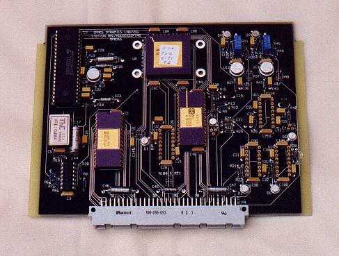
DX ADC/Housekeeping Board Documentation
This board has the least complex of the EDX FPGA's, 'cause you didn't really want to download 50 or 60 pages, did you?
Actel 1020 ADCT&C FPGA Programming Description
                             ADCT&C
         (Analog to Digital Converter Timing & Control)

This chip is programmed to provide the following functions:

     Controls  the  Analog to Digital Converter (ADC) and  analog
multiplexers  to provide on-gimbal temperature and  other  analog
data  to  be sent to the off-gimbal electronics over the A  color
fiber optic downlink.
     Monitors the fiber optic uplink status and sends the  status
to  the  off-gimbal  electronics  via the  A  color  fiber  optic
downlink.

                        ADCT&C IO SIGNALS

                             INPUTS

     TXCLK  (Tansmit CLocK) - Master clock from the RDFC&T  logic
running at the fiber optic downlink TAXI chip rate (7.192 MHZ).

     INTTM[2:0]  (INTegration TiMe 0,  1,  2) - Signals from  the
RDFC&T  logic.   Used to determine the sampling rate in terms  of
scan frames.

     C0A (Control bit 0 A) - Control bit zero to the A color TAXI
transmitter  from RDFC&T.   This bit is set for one clock at  the
end  of every scan frame.   Used to start a conversion and switch
multiplexer inputs every n scan frames,  with n determined by the
integration time.

     NRESET (Not RESET) - True low at power on to initialize  the
counters and sequencing flip-flops.   Used mainly for simulation,
and  could  be  tied to VCC for normal operation  of  this  chip.
However,  it  is  inverted and sent as true high RST to the  ADC.
This  signal is required,  so NESET must be connected  to  system
reset.

     ASTRB  (A STRoBe) - Control strobe from RDFC&T that  strobes
data into the A color TAXI chip transmitter.   Used as a clock to
sequence the ADC ID and data bytes onto the A color downlink data
bus for transmission to the AEU.

     ADCOE  (Analog to Digital Converter Output Enable)  - Signal
from  RDFC&T  enabling the tri-state data outputs to the A  color
TAXI  chip.   Also  used  to  enable ASTRB  to  the  data  output
sequencer.

     SCLK  (Serial data CLocK) - Data clock from the ADC for  the
ADC serial data stream.   ADC serial data is valid on the  rising
edge of this clock.

     SDAT  (Serial  DATa) - Serial conversion data from the  ADC.
Valid on the rising edge of SCLK.

     RXDSTRB  (Receiver Data STRoBe) - Received data strobe  from
the fiber optic uplink TAXI chip receiver.  Used to reset a watch
dog timer to indicate uplink status.

                             OUTPUTS

     ADCCLK  (Analog to Digital Conversion CLock) - TXCLK divided
by two.  Used as ADC conversion clock.

     STRTCONV  (STaRT  CONVersion) - Signal to the ADC to  sample
and hold input and start the current conversion.

     DGA[3:0] (DG535 multiplexer Address 0 thru 3) - Input select
signals to the Siliconix Incorporated DG535 multiplexer chip.

     HSA[3:0]  (HS-1840RH  multiplexer Address 0 thru  3)  - Input
select signals to the Harris HS-1840RH multiplexer chip.

     RST (ReSeT) - Reset signal true high to the  ADC.   Inverted
NRESET.

     D[7:0]  (Data  0 thru 7) - Tri-state data outputs to  the  A
color  TAXI transmitter.   ADC data are enabled and  output  from
these outputs under control of the RDFC&T and ADCT&C logic.

                            ADCCNTRL
              (Analog to Digital Converter CoNTRoL)

     This module controls the sample rate of the ADC conversions.
Due  to  the  settling  time of the noise filtering  on  the  ADC
inputs,  sampling once every RASP scan at the faster  integration
times  would result in inaccurate readings when switching between
multiplexer inputs that have large differences.  By sampling once
every  eight scans,  four scans,  two scans,  and every scan  for
integration times of one, two, three, four and five respectively,
the  sampling  rate is limited to 2.576 msec  minimum.   This  is
enough  time  to  allow  step input  changes  to  settle  at  the
converter input before being converted.
     The  scans are counted using the three bit ripple counter by
using  the C0A signal that is produced by the RDFC&T  logic  once
per  scan  at  the  end  of each scan  as  a  count  clock.   The
appropriate count decode for mod 8, 4, 2, or 1 is selected by the
four  to  one mux under control of the integration  time  command
inputs from the RDFC&T.   After the rising edge of C0A clocks the
ripple  counter,  the  falling  edge of the  signal  latches  the
settled decode output from the mux.  The decode is syncronized to
the  master  clock and guarded against metastability by  the  two
flip-flops on the output of the decode latch flip-flop.
     The  latched  decode  enables the two bit  counter  that  is
initially at zero.   At count equals two,  the STRTCONV strobe is
generated.   This strobe to the ADC samples and holds the current
ADC input, and starts the conversion process.  The strobe is also
used  internally  to reset the ADC data receiver  shift  register
logic in preparation for receipt of the new conversion.
     After the start of the conversion, at the count of three the
INCADD  signal  goes  true,  enabling the five  bit  mux  address
generator counter for one clock to set up the inputs for the next
conversion.   This  can be done before the started conversion  is
complete,  because the ADC has held the conversion input when the
STRTCONV signal went true.
     The  next  clock  sends the three decode back to  the  clear
inputs  of the counter and the enable latches.   This leaves  the
system in state zero waiting for the next C0A/INTTM true to start
the next conversion and input increment sequence.

NOTE:  Since  the  sample rate is less than the scan rate at  the
three  fastest integration times,  duplicate ADC data is sent  in
the downlink frames when a new conversion has not been initiated.

                              ADCSR
          (Analog to Digital Converter Shift Register)

     Because  the low skew clock network is needed for the  other
functions of the ADCT&C logic, the serial data clock from the ADC
must  use the standard unpredictable skew chip nets.   The  ADCSR
module  uses a ripple downcounter with a 1 of 16 decode to enable
the correct flip-flop latch to capture the conversion serial data
output.   The STRTCONV signal from the ADCCNTRL module resets the
ripple count to F, and the falling edge of the first serial clock
(the  inactive state of SCLK is high) decrements the count to  E,
enabling the Q15 flip-flop.   The rising edge of the first serial
clock  then  latches  the MSbit of the converision into  the  Q15
flip-flop.   The  falling edge of the next clock  decrements  the
count  to  D,  and  the next clock rising edge latches  the  next
significant bit.  This process repeats for the 16 conversion bits
of each conversion.   After all bits are received, the conversion
is held in these latches for transmission to the AEU.

                             ADCMUX
           (Analog to Digital Converter MUltipleXers)

     This  module simply contains eight 4-input multiplexers that
under control of the select lines are used to present the correct
ID/data byte at the appropriate time for transmission to the AEU.

                          ADCCLK LOGIC

     The flip-flop whose output provides the ADCCLK output simply
divides the master clock (TXCLK) clock by two.  This is necessary
since  the  7  plus MHZ rate of the  TXCLK  exceeds  the  maximum
operating  frequency  of the analog to  digital  converter.   The
3.596  MHZ  rate of the ADCCLK output is comfortably  within  the
operating frequency range of the CRYSTAL 5016 ADC chip.

              INPUT MULTIPLEXERS ADDRESS GENERATION

     The  five  bit  mux address counter  increments  once  every
eighth,  fourth,  second, or every RASP scan as determined by the
INCADD  output of the ADCCNTRL module.   Using the MSb to  modify
the output addresses, the following address select results:


   Count  HSA  DGA  Downlink ID           Input

     0     0    0        1         Fore Baffle Temperature
     1     0    1        2         Cryo Tank Temperature #1
     2     0    2        3         Cryo Tank Temperature #2
     3     0    3        4         Scan Mirror Temperature
     4     0    4        5         Scan Mirror Motor Temperature
     5     0    5        6         Cryo Tank Fill Temperature #1
     6     0    6        7         Cryo Tank Fill Temperature #2
     7     0    7        8         Quick Disconnect Fill Temp. #1
     8     0    8        9         Quick Disconnect Fill Temp. #2
     9     0    9        A         M1 Mirror Temperature
     A     0    A        B         M2 Mirror Temperature
     B     0    B        C         M3 Mirror Temperature
     C     0    C        D         Analog GND
     D     0    D        E         Analog GND
     E     0    E        F         Analog GND
     F     0    F       10         Analog GND
    10     0    0       11         Fore Baffle Temperature
    11     1    0       12         Rear Baffle Temperature #1
    12     2    0       13         Rear Baffle Temperature #2
    13     3    0       14         FPA Mount Temperature #1
    14     4    0       15         FPA Mount Temperature #2
    15     5    0       16         Cryo Pressure
    16     6    0       17         RDF Box Temperature
    17     7    0       18         Scan Mirror Preamp Temperature
    18     8    0       19         Analog GND
    19     9    0       1A         Analog GND
    1A     A    0       1B         Analog GND
    1B     B    0       1C         Analog GND
    1C     C    0       1D         Analog GND
    1D     D    0       1E         Analog GND
    1E     E    0       1F         Analog GND
    1F     F    0        0         Fore Baffle Temperature

                    ADCMUX SELECT GENERATION

     The  two  flip-flops  in  the  center  left  of  the  ADCT&C
schematic  are a two bit ripple counter with the inverted  (true)
outputs connected to the ADCMUX.   The C0A signal marking the end
of  a transmission frame clears the count to be ready to send the
ADC  data.   The ADCOE signal from the RDFC&T logic  enables  the
zeroeth  ADC  byte  onto the color A transmitter  data  bus,  and
enables the ASTRB signal as a clock to this counter.   The rising
edge  of ASTRB then strobes the byte into  the  transmitter,  and
increments  the  count so that the next ADC byte is presented  to
the  data  bus.   This repeats for the time the  ADCOE  is  true,
successively selecting the ADC data for transmission.  The output
format is as follows:

     Byte 0 -  ID and Uplink Status
               bit 0 thru bit 5 - Sample ID
               bit 5 - Uplink status, 1=OK, 0=NOK
     Byte 1 -  ADC reading LSB
     Byte 2 -  ADC reading MSB
     Byte 3 -  Spare, Always FF

                  UPLINK STATUS WATCH DOG TIMER

     The  4 bit counter at the lower left of the ADCT&C schematic
is  constantly being reset by the Data STRoBe (DSTRB) signal from
the  fiber optic uplink TAXI chip receiver.   If the DSTRB's  are
absent for 15 or more TXCLK cycles,  the timer times out, holding
a  zero  on  the  uplink status decode until  a  DSTRB  is  again
received.