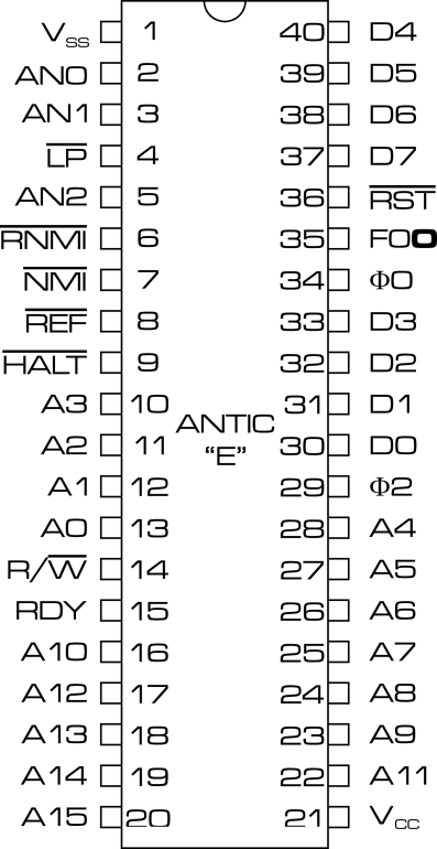
ANTIC Pinout Diagram

A vector graphic pinout is also available in
Encapsulated PostScript format.
Key
- A0-A15: Memory address bus
- D0-D7: Memory data bus
- AN0-AN2: CTIA/GTIA bus (data type unknown)
- Vss: Ground
- LP: Light pen input
- RNMI: Non-maskable interrupt input
- NMI: Non-maskable interrupt output (to CPU)
- REF: RAM refresh output
- HALT: Halt output; suspends the CPU while ANTIC reads memory
- R/W: Read/write direction
- RDY: ANTIC pulls this pin low to halt the CPU when the WSYNC
register is written, until the next horizontal blank occurs.
- Vcc: +5V power
- Ø2: Phase 2 input clock
- Ø0: Phase zero clock output
- FØ0: Fast phase 0 input clock
- RST: Resets ANTIC
Note: The information here is more fully documented in Atari's
technical documents.


 Back to Atari Technical Information page