FEATURES
|
|  | | 20us (PA-AD12), 10us (PA-AD12-H) analog to digital (A/D) converter.
| | | 12-Bit A/D converter with 1 LSB accuracy.
| | | 8 differential or 16 single-ended analog input channels.
| | | 8254 timer provides background A/D conversion.
| | | Jumper-configuration gain controller.
| | | DC/DC converter to reduce noise from PC.
|
DESCRIPTION
|
For users who require A/D only, we've got a card for you. The PA-AD12
and PA-AD12-H are 12 bit analog to digital converters.
The PA-AD12 and PA-AD12-H have 8 differential/16 single-ended input
channels with 12 bit 20us/10us A/Ds. An 8254 Timer/Counter, on board,
allows background conversions.
This module also comes with jumper-configurable gain control that
allows the user to select the gain.
|
MODEL NUMBER
| Function | PA-AD12 | PA-AD12-H
|
|---|
| A/D | Resolution | 12 Bit | 12 Bit
| | Channels | 8 Differential or 16 Single-ended | 8 Differential or 16 Single-ended
| | Conversion time | 20 us | 10 us
| | Accuracy | 11 Bit | 11 Bit
|
THE EXPANSION OPTIONS
| Model No. | Function
|
|---|
| ST-DM37 | Screw terminal board for A/D D/A connector
| | IC-XCXD | Chassis for XCI/XDI expansion cards
|
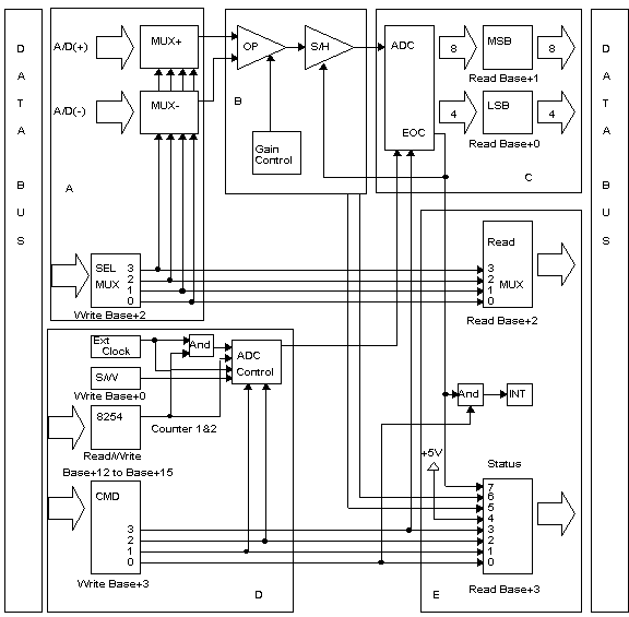
SYSTEM BLOCK DIAGRAM
FUNCTIONAL DESCRIPTION
|
The signal connector - The signal connector is a 37 pin D-type male connector.
A/D channel selection - The PA-AD12(-H) can be configured for 8 differential inputs or 16 single-ended inputs. The configuration is set by an on-board
jumper, the channel is software selectable. (base+2 port)
Sample and hold - The PA-AD12(-H) uses a sample and hold circuit that depends on the end of conversion
signal from the A/D chip. Thus, the sample and hold rate is a function of the A/D conversion speed.
A/D conversion control -
The A/D conversion can be triggered in three ways, they can be selected by writing a command to the A/D command port
(base+3).
Trigger method 1 : S/W trigger conversion
This method of conversion is very easy to implement because the software is directly
controlling the A/D conversions.
Trigger method 2 : External clock conversion
The external clock conversion consists of using an external clock or pulse, longer than 200 nanoseconds,
to trigger the A/D conversion. This gives the user great flexibility in providing
a trigger signal that enables one to synchronize the A/D with other devices.
Trigger method 3 : 8254 timer conversion
Timer conversion use the 8254 to generate a clock pulse that enablesconversion to be done in the background leaving
the CPU to do more important tasks.
A/D conversion
When an A/D conversion takes place, (by software trig,
external clock trig, etc.) the EOC (End Of Conversion) line
goes high. Once the signal is received, conversion of the voltage
held by the sample and hold unit is initiated. Once the converison
is initiated (EOC is high), no other start conversion command
will be accepted until the completion of the conversion.
Upon completion of the conversion, the EOC
line goes low (in timer or external clock trig mode, an interrupt
will occurred). Next, the least significant byte (LSB) and the most
significant byte (MSB) of the digital value for the voltage can be
read from the data registers, base+0 and base+1 respectively.
The 8 bits of the base+1 port are the 8 most significant
bits of the A/D conversion result. The 4 most significant bits of
the base+0 port are the 4 least significant bits of the A/D conversion
Reading conversion result -
The conversion status of the A/D can be read from the status port.
|
REGISTER INFORMATION
| Port | Default | Direction | Function
|
|---|
| +0 | 02E0H | I/O read | A/D LSB data
| | I/O write | Start A/D conversion
| | +1 | 02E1H | I/O read | A/D MSB data
| | I/O write | None
| | +2 | 02E2H | I/O read | A/D channel select
| | I/O write
| | +3 | 02E3H | I/O read | A/D status
| | I/O write | A/D command
| | +12 | 02ECH | I/O read | 8254 counter 0 data (A/D internal use)
| | I/O write
| | +13 | 02EDH | I/O read | 8254 counter 1 data (A/D timer conversion)
| | I/O write
| | +14 | 02EEH | I/O read | 8254 counter 2 data (A/D timer conversion)
| | I/O write
| | +15 | 02EFH | I/O read | 8254 read-back status
| | I/O write | 8254 command
|
PROGRAMMING INFORMATION
|
Shipped with this board are Utility, Library and Sample Programs.
These programs are included with the product at no additional expense.
Utility Program -
This program will provide comprehensive testing of various functions
of the board to ensure proper operation.
Library And Sample Programs -
The library program provides the interface to Turbo-C, Microsoft Quick
Basic, Microsoft Quick C, Microsoft GW-BASIC, IBM BASIC and Assembler.
Labtech Notebook Driver -
A Labtech's Notebook driver interface is available as an optional product.
Window Driver -
Window 3.1 and Window NT driver interface is available as an optional product.
|
Specifications
| Analog Inputs (A/D)
|
|---|
| Resolution | 12 bits
| | Input channel | 16 channels (single-ended)
| | 8 channels (differential)
| | Input voltage range | -5V to +5V, -10Vto +10V
| | 0V to +5V, 0V to +10V
| | Accuracy | 1 bit
| | Conversion time | 20us(PA-AD12)
| | 10us (PA-AD12-H)
| | Overvoltage | 35V
| | Gain controller | 1, 2, 5, 10, 20, 50 or user define
by H/W jumper setting
| | Conversion method | S/W trig
| | External clock trig
| | Internal 8254 timer trig
| | Connector | 37 pins D-type male connector
| | Counter Timer (CLK)
|
|---|
| Controller | 8254
| | Counters | 3 16-bit down counter
| | 2 for A/D timer conversion
| | 1 for user's application
| | Clock source | 4 MHz
| | Input/output type | TTL
| | Interface Characters
|
|---|
| Compatible bus | IBM PC and compatibles
| | Data path | 8 bits
| | Interface type | 12 Bit I/O mapped
| | I/O location occupied | 8
| | Port address range | 100H to FF0H
| | Interrupt | IRQ2,3,4,5,7,10,11,12,14,15
| | Interrupt source | A/D end of conversion (EOC)
| | Power requirement | 1.25A / +5V
| | Physical/Environmental
|
|---|
| Operating temperature | +5 ° C to +50 ° C
| | Humidity | 0 to 90% non-condensing
| | Weight | 175 g
| | Dimension | 17.5 x 12.6 x 2.0 cm
|
|