Acqutek - PA-CP12 (details)
Home - Product Index - Contact & Ordering - Support - Calendar - Download - Y2K - Clearance

Similar / Related Products PI-IO48A - PA-CP12 - PA-ST12(-H) - PA-MA12(-H) - PA-MD12(16) - PA-AD12(-H) - PA-DA12(16)
XC-IO96 - XC-AD12 - XC-DA12
XI-PI08 - XI-IM04 - XO-RR08 - XO-SRD4/XO-SRA4 - ST-XD02 - ST-DM37 - IC-XCXD

PA-CP12 Brief Description
Low Cost Multi-I/O card (A/D D/A & Digital I/O)

Description - Model No - Expansion - Block Diagram - A/D - D/A - I/O - Register - Programming - Specifications

FEATURES

    12 bit, 200 us analog to digital (A/D) convertor.
    16 single-ended analog inputs.
    8254 timer provides background conversion.
    12 bit, 20 us digital to analog (D/A) convertor.
    One voltage output.
    8 digital inputs.
    8 digital outputs.

DESCRIPTION

    Let's face it - not everyone needs a high-speed, high-accuracy A/D D/A card. So why should everyone have to pay full price for these functions. The answer is simple -- they shouldn't. This is why we created the PA-CP12: for the simple A/D, D/A and digital I/O applications. It is the affordable solution.

    The PA-CP12 is a 16 single-ended input, 12 bit 200us A/D converter, 1 voltage output, 20us D/A card with an 8254 timer on board which generates an accuracy signal for A/D background conversion.

    The board also comes with an 8 bit in 8 bit out digital I/O. Various expansion models like S.S.R. O/P, reed relay O/P, photo-coupled I/P, and screw terminal boards are also available for the PA-CP12.

MODEL NUMBER

    Function PA-CP12
    A/D Resolution 12 Bit
    Channels 16 Single-ended
    Conversion time200 us
    D/A Resolution12 Bit
    Channels1
    Conversion time20 us
    Digital I/ODigital I/P8 Bit
    Digital O/P8 Bit

THE EXPANSION OPTIONS

    Both inputs and outputs, have optional expansion modules (daughter cards) that extend the I/O for interfacing operations. These modules are called XDI expansion boards and include options like reed-relay output modules or photo-coupled input modules. The PA-CP12 could support one input card and one output card totaling 16 individual lines in all (half input/half output). For more information on XDI expansion boards, see the expansion product section.

    Model No. Function
    XI-PI08 3-32V photo-coupled input expansion
    XI-IM04-32 12-32V AC/DC input expansion
    XI-IM04-140 90-140V AC/DC input expansion
    XI-IM04-280 180-280V AC/DC input expansion
    XO-RR08 10VA reed relay output expansion
    XO-SRD4 3A 5-60V DC S.S.R. output expansion
    XO-SRA4 3A 24-280V AC S.S.R. output expansion
    ST-XD02 2 XDI screw terminal board
    ST-DM37 Screw terminal board for A/D D/A connector
    IC-XCXD Chassis for XCI/XDI expansion cards

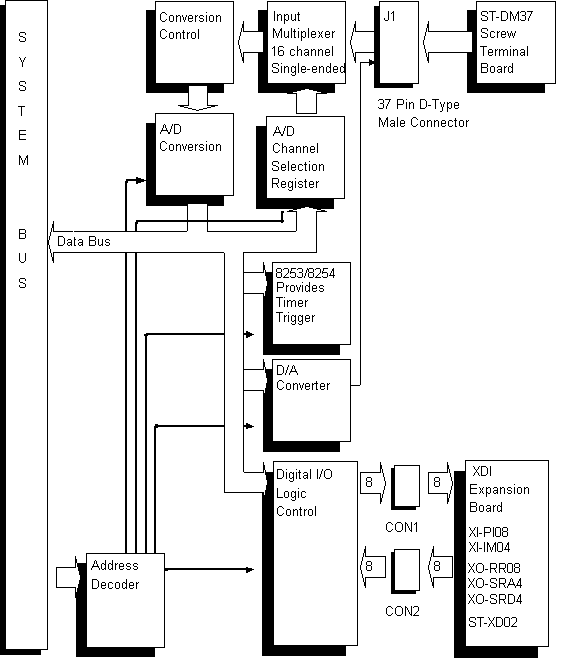
SYSTEM BLOCK DIAGRAM

FUNCTIONAL DESCRIPTION

    Analog Input (A/D)

    The PA-CP12 provides 16 single-ended channels, of 12 bit, 200us analog to digital conversion.
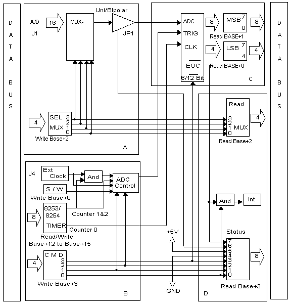
    The signal connector - The analog input signal connector is a 37 pin D-type male connector.

    A/D channel selection - The PA-CP12 is configured for 16 single ended inputs only. Writing to base+2 port selects the channel that is to be converted.

    Sample and hold - The PA-CP12 does not provide a sample and hold circuit.

    A/D conversion control - The A/D conversion can be triggered in three ways, they are selected by programming the command port base+3.

      Trigger method 1 : S/W trigger conversion
      This method of conversion is very easy to implement because the software is directly controlling the A/D conversions. The conversion will be started by writting any data to the S/W trigger port (base+0).
      Trigger method 2 : External clock conversion
      The external clock conversion consists of using an external clock or pulse (coming in from a jumper) to trigger the A/D conversion. This gives the user great flexibility in synchronizing the A/D with other devices.
      Trigger method 3 : 8254 timer conversion
      The 8254 timer conversion method uses the 8254 timer controller to generate an accurate time pulse which triggers the start of conversions. An option that goes with this is to gate the 8254 timer trigger signals with an external signal. This gives the user external control over A/D conversions using the 8254 timer.

    A/D conversion - When an A/D conversion takes place, the EOC (End of conversion) line goes high. Once the start conversion signal is received, conversion of the voltage at the selected channel is initiated. Once the conversion is initiated, no other start conversion command will be accepted until the completion of the conversion. Upon completion of the conversion, the EOC line goes low (in timer or external clock trig mode, an interrupt will occur). Next, the least significant byte (LSB) and the most significant byte (MSB) of the digital value for the voltage can be read from the data registers, base+0 and base+1 respectively.

    Reading conversion result - There are two methods to read the conversion result :

      Method 1 : Polling the EOC status
      This method is the simplest method to do A/D conversions and read the data. However this method ties up the CPU because one must keeping polling the EOC bit in the status register so that one can know when an A/D conversion is completed.
      Method 2 : Interrupt
      This method is more efficient than polling the EOC status, because upon a completed conversion, the PA-CP12 interrupts the CPU to read the conversion result. In other words, the conversion is done in the background, leaving the CPU to do more important tasks.

    Conversion status - The A/D status can be read from two ports; The base+3 port contains the critical information for the setup and condition of the A/D while the base+2 port contains information on the selected channel.

    Analog Output (D/A)

    The PA-CP12 provides one voltage output channel with 12 bit 20us digital to analog conversion.
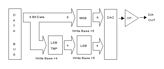
    Data register - The PA-CP12 uses 2 data registers or ports. The ports are base+4 and base+5. Using 2 ports enables the user to send a 12-bit word to the D/A converter using an 8-bit bus without getting glitches on the output. Here is an example of the data register scheme. Say a user wishes to convert the digital value from 1AFH to 1B0H to an analog value. Using the standard approach of sending 8 bits at a time would result in a glitch on the output at these digital values-- 1AFH-1A0H-1B0H (sending LSB first, then MSB) or 1AFH-1BFH-1B0H (sending MSB first, then LSB). However, using the PA-CP12, one would write the 0H (4 least significant bits) to the temporary register (base+4). Next the user would write 1BH (8 most significant bits) to the output port (base+5). Upon writing the MSB to base+5, the data in the temporary LSB register is automatically sent to the output, thus, both MSB and LSB arrive at the D/A simultaneously. (i.e. no glitch)

    D/A conversion - D/A conversion is accomplished using a 12 bit D/A conversion chip. The 12-bit words are sent from the data bus and a temporary register simultaneously. This enables a 12-bit word to be sent from an 8-bit data bus without getting odd glithes on the output.

    The signal connector - The connector for the D/A output signal is the same 37 pin male D-type connector used for the A/D. The A/D and the D/A share the same connector.

    Digital I/O

    The PA-CP12 provides 16 lines of digital I/O; 8-bit digital output and 8-bit digital input.
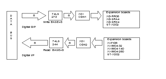
    Digital output - Digital output consists of one 8-bit dedicated output path. To write data out of this path a user simply writes to the I/O ports; base+8 is the output port for CON1.

    Digital input - Digital input consists of one 8-bit dedicated input path. To read data from this path a user simply reads from the I/O ports; base+8 is the input port for CON2.

    The digital I/O connectors - There are two connectors for the digital I/O. Each consists of a 20 pin box header. Connector 1 (CON1) is output and connector 2 (CON2) is input.

REGISTER INFORMATION

    PortDefaultDirectionFunction
    +0 02E0HI/O readA/D LSB data
    I/O writeStart A/D conversion
    +1 02E1HI/O readA/D MSB data
    I/O writeNone
    +2 02E2HI/O readA/D channel select
    I/O write
    +3 02E3HI/O readA/D status
    I/O writeA/D command
    +4 02E4HI/O readNone
    I/O writeD/A LSB data
    +5 02E5HI/O readNone
    I/O writeD/A MSB data
    +8 02E8HI/O readDigital I/P (XDI, CON2)
    I/O writeDigital O/P (XDI, CON2)
    +12 02ECHI/O read8254 counter 0 data (A/D internal use)
    I/O write
    +13 02EDHI/O read8254 counter 1 data (A/D timer conversion)
    I/O write
    +14 02EEHI/O read8254 counter 2 data (A/D timer conversion)
    I/O write
    +15 02EFHI/O read8254 read-back status
    I/O write8254 command

PROGRAMMING INFORMATION

    Shipped with this board are Utility, Library and Sample Programs. These programs are included at no additional expense with this product.

    Utility Program - This program will provide comprehensive testing of various functions of the board to ensure proper operation.
    Library And Sample Programs - The library program provides the interface to Turbo-C, Microsoft Quick Basic, Microsoft Quick C, Microsoft GW-BASIC, IBM BASIC and Assembler.
    Labtech Notebook Driver - A Labtech's Notebook driver interface is available as an optional product.
    Window Driver - Window 3.1 and Window NT driver interface is available as an optional product.

Specifications

    Analog Inout (A/D)
    Resolution / Channel 12 Bits / 16 single-ended
    Input voltage range -5V to +5V, -10V to +10V
    0V to +5V, 0V to +10V
    Accuracy 2 Bits
    Conversion time 200us
    Overvoltage 35V
    Conversion method S/W trig
    External clock trig
    Internal 8254 timer trig
    Connector 37 pins D-type male connector
    Analog Output (D/A)
    Resolution / Channel 12 Bits / 1 voltage output
    Output voltage range -5V to +5V, -10V to +10V
    0V to +5V, 0V to +10V
    Accuracy 2 Bits
    Conversion time 20us
    Connector 37 pins D-type male connector
    Digital I/O (D I/O)
    Number of digital input 8 Bits
    Input type 74LS244
    Input high/low voltage 2.0V/0.8V
    Number of digital output 8 Bits
    Output type 74LS273
    Output high/low voltage 2.4V/0.5V
    Digital I/O connector 2 XDI connectors 20 pins dual-in-line male box header
    Timer (Counter)
    Controller 8254
    Counters 3 16-Bit down counter
    2 for A/D timer conversion
    1 for A/D internal use
    Clock source 4 MHz
    Input/output type TTL
    Interface Characters
    Compatible bus IBM PC and compatibles, 8 Bit Data
    Interface type 12 Bit I/O mapped, 16 I/Os, 100H-FF0H
    Interrupt IRQ2,3,4,5,7,10,11,12,14,15
    Interrupt source A/D end of conversion (EOC)
    Power requirement 460mA / +5V
    100mA / +12V, 100mA / -12V
    Physical/Environmental
    Operating temperature +5 ° C to +50 ° C
    Storage temperature -25 ° C to +85 ° C
    Humidity 0 to 90% non-condensing
    Weight 170 g
    Dimension 17.5 x 12.6 x 2.0 cm

Copyright © 1996 - 2000 by Acqutek Corporation, Inc.