FEATURES
 | | DMA data transfer digital to analog card (D/A).
| | | 12 bits converter. (PA-MD12)
| | | 100 KHz digital to analog converter. (PA-MD12)
| | | 50 KHz digital to analog converter. (PA-MD16)
| | | 16 bits conversion. (PA-MD16)
| | | 2 voltage and current analog inputs.
|
DESCRIPTION
|
The PA-MD12(16) is our DMA transfer D/A card for the
user that needs fast and reliable data transfers which do not rely
This high speed converter performs conversion and
transfers data using DMA; direct memory transfer. This ensures fast
background conversions regardless of the specific computer in use.
This card provides 2 channels of 12 bit or 16 bit digital to analog
conversion (D/A). The conversion time for PA-MD12 is 10 us and 20us
for the PA-MD16. Because this card uses the DMA data transfer, no
matter what kind of CPU you use, the conversion speed is always the
same. (For the PA-MD12 it is 100KHz, for the PA-MD16 it is 50KHz)
The PA-MD12(16) uses an 8254 timer controller to generate conversion
trigger signals. This gives the conversion time more accuracy. The
PA-MD12(16) provides the high speed DMA transfer. However, traditional
conversion methods are also provided for compatibility purposes
|
MODEL NUMBER
| Function | PA-MD12 | PA-MD16 |
|---|
| D/A | Resolution | 12 Bit | 12 Bit
| | Channels | 2 | 2
| | Conversion time | 10 us | 20 us
| | Accuracy | 11 Bit | 14 Bit
|
THE EXPANSION OPTIONS
| Model No. | Function
|
|---|
| ST-DM37 | Screw terminal board for A/D D/A connector
| | IC-XCXD | Chassis for XCI/XDI expansion cards
|
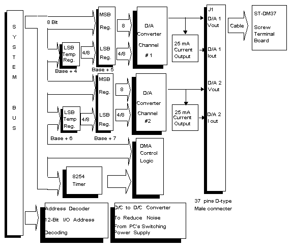
SYSTEM BLOCK DIAGRAM
FUNCTIONAL DESCRIPTION
|
The PA-MD12 provides two voltage and current outputs for 12 bit/16
bit 10us/20us digital to analog conversions.
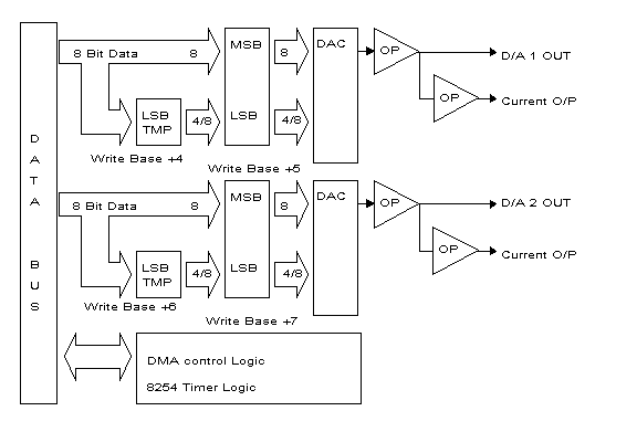
Data register -
The PA-MD12 uses 4 I/O ports to control D/A conversions. The ports are base+4 through
base+7. Using 2 ports per channel enables the user to send a 12-bit word to the D/A
converter using an 8-bit bus without getting glitches on the output. Here is an example
of the data register scheme. Say a user wishes to convert the digital value from 1AFH
to 1B0H to an analog value. Using the standard approach of sending 8 bits at a time
would result in a glitch on the output at the digital values 1AFH-1A0H-1BFH(sending LSB
first, then MSB) or 1AFH-1BFH-1B0H (sending MSB first, then LSB). However, using the
PA-ST12(-H) one would write the 0H (4 least significant bits) to the temporary register
(base+4 for channel one and base+6 channel 2). Next the user would write 1BH (8 most
significant bits) to the output port (base+5 for channel 1 and base+7 for channel 2).
Upon writing the MSB to base+5, the data in the temporary register is automatically
sent to the output, thus, both MSB and LSB arrive at the D/A simultaneously (i.e. no glitch).
D/A conversion -
D/A conversion is accomplished using a 12 bit D/A
conversion chip. The 12-bit words are sent from the data bus and a
temporary register simultaneously. This enables a 12-bit word to be
sent from an 8-bit data bus without getting odd glitches on the output.
DMA Data Transfer -
The DMA transfer is the best way to do the D/A conversion.
Using DMA transfer not only gives the fastest conversion speeds but
also does the conversions in the background leaving the CPU free to
do more important jobs.
The signal connector -
The connector for the D/A output signals is the 37
pin male D-type connector. A screw terminal board and a chassis for
the screw terminal board are available.
|
REGISTER INFORMATION
| Port | Default | Direction | Function
|
|---|
| +4 | 02E4H | I/O write | D/A output 1 LSB data register
| | +5 | 02E5H | I/O write | D/A output 1 MSB data register
| | +6 | 02E6H | I/O write | D/A output 2 LSB data register
| | +7 | 02E7H | I/O write | D/A output 2 MSB data register
| | +8 | 02E8H | I/O write | D/A command
| | +8 | 02E8H | I/O write | D/A status port
| | +9 |
+11 02E9H
02EBH | I/O Read
I/O write | 8254 Timer
|
PROGRAMMING INFORMATION
|
Shipped with this board are Utility, Library and Sample Programs.
These programs are included with the product at no additional expense.
Utility Program -
This program will provide comprehensive testing of various functions
of the board to ensure proper operation.
Library And Sample Programs -
The library program provides the interface to Turbo-C, Microsoft Quick
Basic, Microsoft Quick C, Microsoft GW-BASIC, IBM BASIC and Assembler.
Window Driver -
Window 3.1 and Window NT driver interface is available as an optional product.
|
Specifications
| Analog Output (D/A)
|
|---|
| Resolution | 12 bits (PA-MD12)
| | 16 bits (PA-MD16)
| | Channel | 2
| | Output voltage range | -5V to +5V, -10V to +10V
| | 0V to +5V, 0V to +10V
| | Output current range | -25mA to +25mA
| | 0mA to +25mA
| | Accuracy | 1 bit (PA-MD12)
| | 2 bits (PA-MD16)
| | Conversion time | 10 us,100KHz (PA-MD12)
| | 20 us, 50KHz (PA-MD16)
| | Connector | 37 pins D-type male connector
| | Counter Timer (CLK)
|
|---|
| Controller | 8254
| | Counters | 2 for D/A timer conversion
| | Clock source | 4 MHz
| | Input/output type | TTL
| | Interface Characters
|
|---|
| Compatible bus | IBM PC and compatibles
| | Data path | 8 bits
| | Interface type | 12 Bit I/O mapped
| | I/O location occupied | 8
| | Port address range | 100H to FF0H
| | Interrupt | IRQ2,3,4,5,7,10,11,12,14,15
| | DMA | DREQ0, 1, 3
| | Power requirement/consumption | 600mA / +5V
| | 60mA /+12V and -12V
| | Physical/Environmental
|
|---|
| Operating temperature | +5 ° C to +5 ° C
| | Storage temperature | -25 ° C to +85 ° C
| | Humidity | 0 to 90% non-condensing
| | Weight | 210 g
| | Dimension | 23.5 x 12.6 x 2.0 cm
|
|