|
XCI expansion module connecter -
The Expansion Control Interface (XCI) is designed for the
future expansion of the XCI mother board (PI-IO48 or XU-i088).
The XCI mother board (PI-IO48 or XU-i088) has the capacity to
be connected to up to seven XCI daughter boards using the XCI
bus.
A user simply plugs the XCI cable into the 40 pin dual-in-line
box header connecter on XCI mother board (PI-IO48 or XU-i088)
and the 40 pin plug connecter of daughter cards (XC-DA12).
Please note that the XCI cable for PI-IO48(A) and XU-i088(A)
is different.
The XCI daughter cards (XC-IO96, XC-AD12 and XC-DA12) are
connected to the XCI mother board (PI-IO48) by a 2 feet XCI
cable that is supplied with XCI mother board (PI-IO48 or
XU-i088).
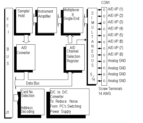
The signal connector -
The signal connecter for A/D signals input is a screw terminal
block (14AWG).
A/D simultaneous S/H -
A simultaneous S/H kit (MK-XC-SH08) is available as an option
product, a user can purchase it from Acqutek. Install the S/H
chips in sockets U30-U43 then adjust JP30A-JP43A to
simultaneous S/H position.
A/D channel selection -
The XC-AD12(-H) is configurred as single ended inputs only.
The channel is software selectable. The port used for channel
selection is base+2. The input channels feed the multiplexers
(8 channels total). Writing to base+2 selects the channel
that is to be converted. The 3 least significant bits (D2-D0)
in base+2 determine the channel that is selected by their
binary equivalents, the D3 determines the simultaneous S/H and
the 4 most significant bits (D7-D5) do not matter. An example
of this is, if one wanted to select the single-ended channel
#6, one would write 0000 x110B to base+2.
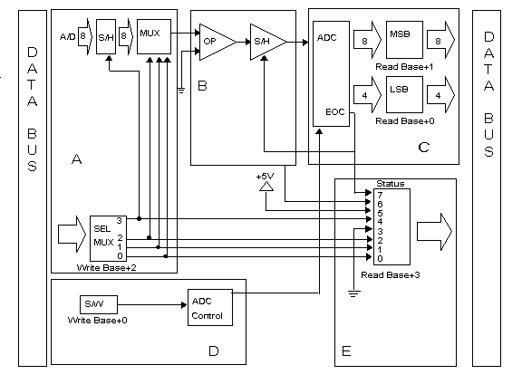
Sample & hold -
The XC-AD12(-H) uses a sample and hold circuit that depends on
the end of conversion signal from the A/D chip. Thus, the
sample and hold rate is a function of the A/D conversion
speed.
A/D conversion -
When the A/D conversion takes place, (by software trig) the
EOC line goes high. Once the signal is received, conversion
of the voltage held by the sample and hold unit is initiated.
Once the conversion is initiated (EOC goes high), no other
start conversion command will be accepted until the completion
of the conversion. Upon completion of the conversion, the EOC
line goes low. Next, the least significant byte (LSB) and the
most significant byte (MSB) of the digital value for the
voltage can be read from the data registers, base+0 and base+1
respectively. The all 8 bits of the base+1 port are the 8
most significant bits of the A/D conversion result, and the 4
most significant bits of the Base+0 port are the 4 least
significant bits of the A/D conversion result.
A/D conversion control -
The A/D conversion can be triggered by writing any data to
base+0 port. (S/W Trig) This method is very easy to implement
because it is directly controlled by the S/W. However this
method ties up the CPU because one must poll the EOC bit in
the status register to know when one can trigger the A/D.
Reading status -
The status of the A/D can be read from base+3 port. This port
contains the condition of the A/D and the channel currently
selected. Bit 7 represents EOC (end of conversion); bit 6
represents the configuration for either unipolar or bipolar
inputs; bit 5 is always set to high (1); bit 4 is simultaneous
S/H control; bit 3 is always set to zero (0); bit 2-0
represent the A/D channel selected.
The signal connecter -
The signal connecter for D/A output signals is the 3 SIL 14
AWG screw terminal. Be sure to check the pin diagram before
using.
|