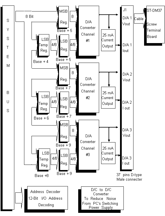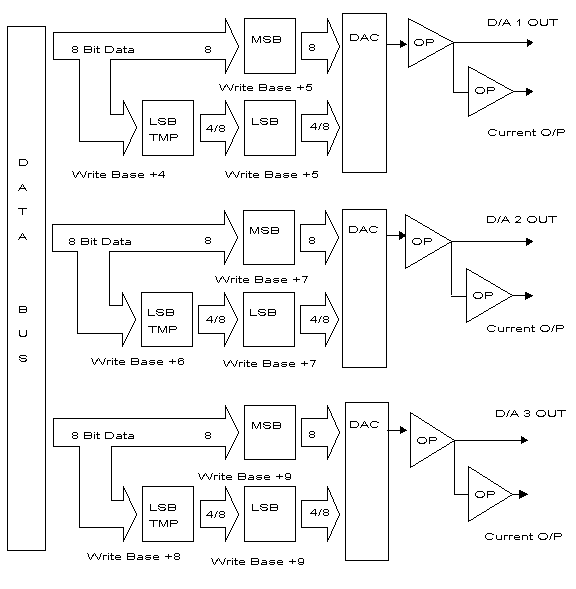
Data register -
The PA-DA12(16) uses 6 data registers or ports. The ports are base+4
through base+9. Using 2 ports enables the user to send a 12-bit or
16-bit word to the D/A converter using an 8-bit bus without getting
glitches on the output.
Here is an example of the data register scheme. Say a user wishes to
convert the digital value from 1AFH to 1B0H to an analog value in the
12-bit D/A conversion. Using the standard approach of sending 8 bits
at a time would result in a glitch on the output at these digital values
1AFH-1A0H-1B0H (sending LSB first, then MSB) or 1AFH-1BFH-1B0H (sending
MSB first, then LSB).
However, using the PA-DA12, one would write the 0H (4 least significant
bits) to the temporary register (base+4 for channel 1, base+6 for channel
2 and base+8 for channel 3). Next the user wouldwrite 1BH (8 most significant
bits) to the D/A O/P (base+5 for channel 1, base+7 for channel 2 and base+9
for channel 3). Upon writing the MSB to base+5, the data in the temporary
register is automatically sent to the output, thus, both MSB and LSB arrive
at the D/A simultaneously. (i.e. no glitch)
D/A conversion -
D/A conversion is accomplished using a 12 or 16 bit D/A conversion chip.
The 12-bit or 16-bit words are sent from the data bus and a temporary register
simultaneously. This enables a 12-bit or 16-bit word to be sent from an 8-bit
data bus without getting odd glitches on the output. (See data register section)
The signal connector -
The connector for the D/A output signals is the 37 pin male D-type connector.
|