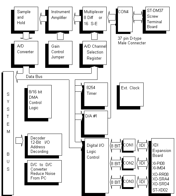
Analog Input (A/D)
The PA-MA12(-H) provides 16 single-ended or 8 differential
channels, 12 bit, 20/10us analog to digital conversion.
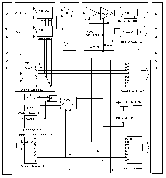
ADC block diagram
The signal connector - The connector for the analog input signals is a 37 pin D-type male
connector. A screw terminal board and a chassis for the screw terminal board are available as optional products.
A/D channel selection - The PA-MA12(-H) can be configured for 8 differential inputs or 16 single ended inputs.
The configuration is set by an on-board jumper. The channel can be selected by writing
the channel limit to channel selection port (base+2).
Sample and hold -
The PA-MA12(-H) uses a sample and hold circuit that depends on the end of conversion
(EOC) signal from the ADC. Thus, the input signal will be held during the conversion.
A/D conversion control -
The A/D conversion can be triggered in three ways.
They are selected by writing the command to the A/D command port (base+3).
Trigger method 1 : S/W trigger conversion
The first type of conversion is software triggered conversion. This method is very easy to
implement because the software is directly controlling the A/D conversions. The conversion
will be started by writting any data to the S/W trigger port (base+0).
Trigger method 2 : External clock conversion
The external clock conversion consists of using an
external clock or pulse, longer than 200 nanoseconds, to trigger the
A/D conversion. The signal comes in from a jumper connection on the
PA-MA12(-H). This gives the user great flexability in providing a
trigger signal that enables one to synchronize the A/D with other
devices.
Trigger method 3 : 8254 timer conversion
The 8254 timer conversion is similar to external triggering except the 8254 timer conversion
uses the 8254 timer controller to generate accurate time pulses to trigger and start the conversions.
An option that goes with this is to gate the 8254 timer trigger signals with the external signal
(from a jumper). In other words, the timer signal and the external signal would be ANDed to give one
external control over A/D conversions with the 8254 timer.
A/D conversion -
When the conversion takes place, the EOC (End
Of Conversion) line goes high, and the input voltage will be held
by the sample and hold circuit. Once the conversion is initiated (EOC
goes high), no other start conversion command will be accepted until
the completion of the conversion.
Upon completion of the conversion, the EOC
line goes low, the least significant byte (LSB) and the most significant
byte (MSB) of the digital value for the voltage will be stored in
a temperary buffer, and the data will not be changed until the completion
of next conversion. The data can be read from the data registers.
Base+0 and base+1 for 8 bit transfer. For the 16 bit transfer, base+0
is also used --16 bit PC bus only.
Upon the end of conversion, the interrupt or DMA request will be issued
depending on the selection for reading conversion results.
Reading conversion result -
The PA-MA12(-H) conversion can be processed by the following methods:
Method 1 : Polling the EOC status
This method is the simplest method to do A/D conversions and read the data. However,
this method ties up the CPU because one must keeping polling the EOC bit in the status
register so that one can know when the A/D conversion is completed.
Method 2 : Interrupt
This method is more efficient than polling the EOC status, because
upon completed conversion, the PA-MA12(-H) interrupts the CPU to read
the conversion result. In other words, the conversion is done in
the background, leaving the CPU to do more important tasks.
Method 3 : DMA Transfer
DMA transfer is the best way to do A/D conversions.
This is because using DMA transfer imparts the fastest conversion
speeds and does the conversions in the background. This leaves the
CPU free to do more important jobs.
Conversion status -
Reading status -
The status of the A/D can be read from two ports; (base+2 and base+3.)
The base+3 port contains critical information for the setup and conditions of the
A/D while the base+2 port contains information on the selected channel.
Maximum conversion speed -
The maximum conversion speed for multi-channel conversions are :
| Conversion Method | PA-MA12 | PA-MA12-H
|
|---|
| Pentium/133 | 80486/100 | 8088/8 | Pentium/133 | 80486/100 | 8088/8
| | Polling EOC | 20KHz | 15KHz | 8Hz | 25KHz | 17KHz | 10KHz
| | Interrupt | 45KHz | 40KHz | 15KHz | 45KHz | 42KHz | 20KHz
| | DMA | 50KHz | 50KHz | 50KHz | 100KHz | 100KHz | 100KHz
|
Analog Output (D/A)
The PA-MA12(-H) provides one voltage output channels 12 bit 10us digital to analog converter.
DAC block diagram -
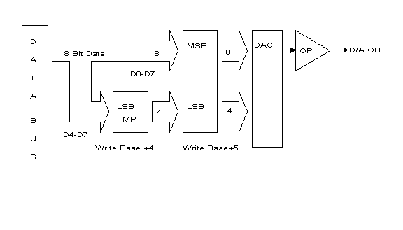
Data register -
The PA-MD12(-H) uses 2 I/O ports to control D/A conversions. The ports are
base+4 through base+7. Using 2 ports per channel enables the user to send
a 12-bit word to the D/A converter using an 8-bit bus without getting glitches
on the output. Here is an example of the data register scheme. Say a user
wishes to convert the digital value from 1AFH to 1B0H to an analog value. Using
the standard approach of sending 8 bits at a time would result in a glitch on
the output at the digital values 1AFH-1A0H-1BFH (sending LSB first, then MSB) or
1AFH-1BFH-1B0H (sending MSB first, then LSB). However, using the PA-ST12(-H) one
would write the 0H (4 least significant bits) to the temporary register (base+4 ).
Next, the user would write 1BH (8 most significant bits) to the output port
(base+5). Upon writing the MSB to base+5, the data in the temporary register is
automatically sent to the output, thus, both MSB and LSB arrive at the D/A
simultaneously (i.e. no glitch).
D/A conversion -
D/A conversion is accomplished using a 12 bit D/A
conversion chip. The 12-bit words are sent from the data bus and a
temporary register simultaneously. This enables a 12-bit word to be
sent from an 8-bit data bus without getting odd glitches on the output.
The signal connector -
The connector for D/A output signals is the same 37 pin male D-type
connector used for the A/D. The A/D and D/A share the same connector.
Digital I/O
The PA-MA12(-H) features a digital I/O controller - 8255. It has 24 digital I/O lines that are divided into three 8-bit
ports. Each port can be programmed as either input or output.
All digital I/Os are configured as Expansion Data
Interface (XDI). A variety isolated I/O expansion boards are available.
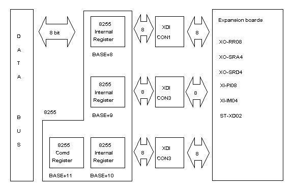
The digital I/O connectors -
There are three connectors for the digital I/O. Each
consists of a 20 pin dual-in-line box header.
|