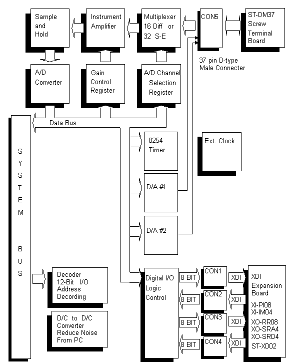
Analog Input
The PA-ST12(-H) provides 32 single-ended or 16 differential
channels of 12 bit, 20/10us analog to digital conversion.
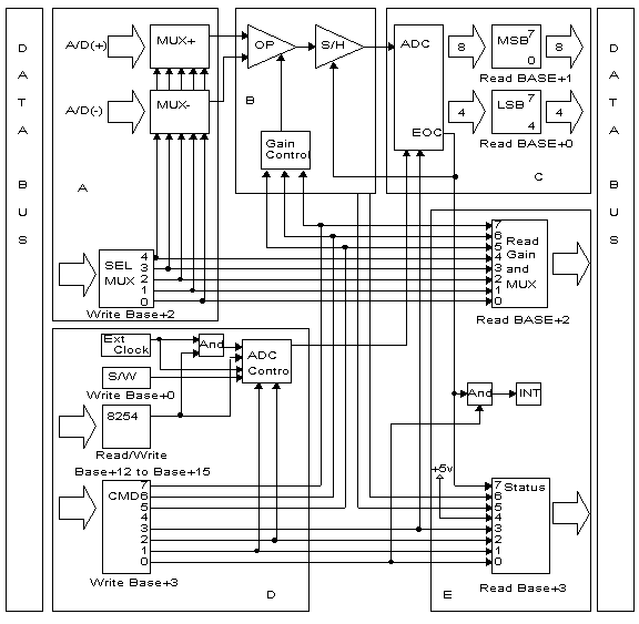 ADC block diagram -
The signal connector - The analog input signal connector is a 37 pin D-type male connector.
A/D channel selection -The PA-ST12(-H) can be configured for 16 differential inputs or 32 single ended inputs. The configuration is set
by an on-board jumper. The channel can be selected by writing to the base+2 port.
Sample and hold -
The input signal will be held during the conversion.
A/D conversion control -
The A/D conversion can be triggered in three ways. They are selected by programming the command port base+3.
Trigger method 1 : S/W trigger conversion
This conversion method is very easy to implement because the software is directly controlling the A/D conversions.
The conversion is started by writting any data to the S/W trigger port (base+0).
Trigger method 2 : External clock conversion
The external clock conversion consists of using an external clock or pulse (coming in from a jumper) to trigger
the A/D conversion. This gives the user great flexibility in synchronizing the A/D with other devices.
Trigger method 3 : 8254 timer conversion
The 8254 timer conversion method uses the 8254 timer controller to generate accurate time
pulses to trigger the start of conversions. An option that goes with this, is to gate the 8254
timer trigger signals with the external signal. This would give the user external control over
A/D conversions using the 8254 timer.
A/D conversion -
When an A/D conversion takes place, the EOC (End Of Conversion) line goes high. Once the start conversion signal
is received, conversion of the voltage at the selected channel is initiated. Once the conversion is initiated,
no other start conversion command will be accepted until the completion of the conversion.
Upon completion of the conversion, the EOC line goes low (in timer or external clock trig mode, an
interrupt will occur). Next, the least significant byte (LSB) and the most significant byte (MSB) of
the digital value for the voltage can be read from the data registers, base+0 and base+1 respectively.
There are two methods to read the conversion result :
Reading conversion result -
There are two methods to read the conversion result :
Method 1 : Polling the EOC status
This method is the simplest method to do A/D conversions and read the data. However, this
method ties up the CPU because one must keep polling the EOC bit in the status register so
that one can know when A/D conversion is completed.
Method 2 : Interrupt
This method is more efficient than polling the EOC status, because upon completed conversion,
the PA-ST12 interrupts the CPU to read the conversion results. In other words,
the conversion is done in the background, leaving the CPU to do more important tasks.
Conversion status -
Reading status
The base+3 port contains the critical information for the setup and condition of the A/D while
the base+2 port contains information on the selected channel and selected gain range.
Analog Output (D/A)
The PA-ST12 provides two voltage output channels of 12 bit 10us digital
to analog conversion.
DAC block diagram -
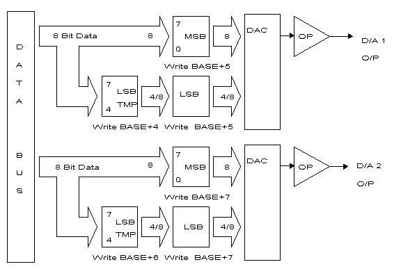
Data register -
The PA-ST12(-H) uses 4 I/O ports to control D/A conversions.
The ports are base+4 through base+7.
Using 2 ports enables the user to send a 12-bit word
to the D/A converter using an 8-bit bus without getting glitches on
the output.
Here is an example of the data register scheme. Say
a user wishes to convert the digital value from 1AFH to 1B0H to an
analog value. Using the standard approach of sending 8 bits at a time
would result in a glitch on the output at the digital values 1AFH-1A0H-1BFH
(sending LSB first, then MSB) or 1AFH-1BFH-1B0H (sending MSB first,
then LSB). However, using the PA-ST12(-H) one would write the 0H (4
least significant bits) to the temporary register (base+4 for channel
one and base+6 channel 2). Next, the user would write 1BH (8
most significant bits) to the output port (base+5 for channel 1 and
base+7 for channel 2). Upon writing the MSB to base+5, the data
in the temporary register is automatically be sent to the output,
thus, both MSB and LSB arrive at the D/A simultaneously. (i.e. no
glitch)
D/A conversion -
D/A conversion is accomplished using a 12 bit D/A
conversion chip. The 12-bit words are sent from the data bus and a
temporary register simultaneously. This enables a 12-bit word to be
sent from an 8-bit data bus without getting odd glitches on the output.
The signal connector -
The signal connector for the D/A output signals is the same 37 pin male D-type
connector used for the A/D. The A/D and the D/A share the same connector.
Optional product
| Model No. | Function
|
|---|
| ST-DM37 | Screw terminal board for A/D D/A
| | IC-XCXD | Chassis for ST-DM37 and XCI/XDI cards
|
Digital I/O
The PA-ST12(-H) provides 32 channels digital I/O;
16-bit digital outputs and 16-bit digital inputs.
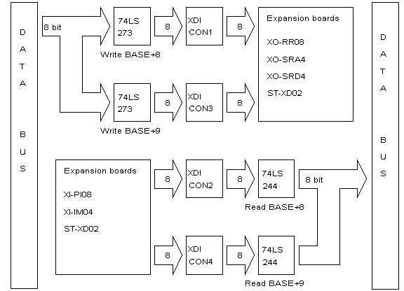
Digital output -
Digital output consists of two 8-bit dedicated output paths. To write data out of these two paths a user
simply writes to the I/O ports; base+8 is the output port for CON1, base+9 is the output port for CON3.
Digital input -
Digital input consists of two 8-bit dedicated input paths. To read data from these two paths a user
simply reads from the I/O ports; base+8 is the input port for CON2, base+9 is the intput port for CON4.
The digital I/O connectors -
There are four connectors for the digital I/O. Each consists of a 20 pin dual-in-line box header.
Connectors 1 and 3 (CON1 & CON3) are output and connectors 2 and 4 (CON2 & CON4) are input.
|