|
XCI expansion module connecter -
The Expansion Control Interface (XCI) is designed for the
future expansion of the XCI mother board (PI-IO48 or XU-i088).
The XCI mother board (PI-IO48 or XU-i088) has the capacity to
be connected to up to seven XCI daughter boards using the XCI
bus.
A user simply plugs the XCI cable into the 40 pin dual-in-line
box header connecter on XCI mother board (PI-IO48 or XU-i088)
and the 40 pin plug connecter of daughter cards (XC-DA12).
Please note that the XCI cable for PI-IO48(A) and XU-i088(A)
is different.
The XCI daughter cards (XC-IO96, XC-AD12 and XC-DA12) are
connected to the XCI mother board (PI-IO48) by a 2 feet XCI
cable that is supplied with XCI mother board (PI-IO48 or
XU-i088).
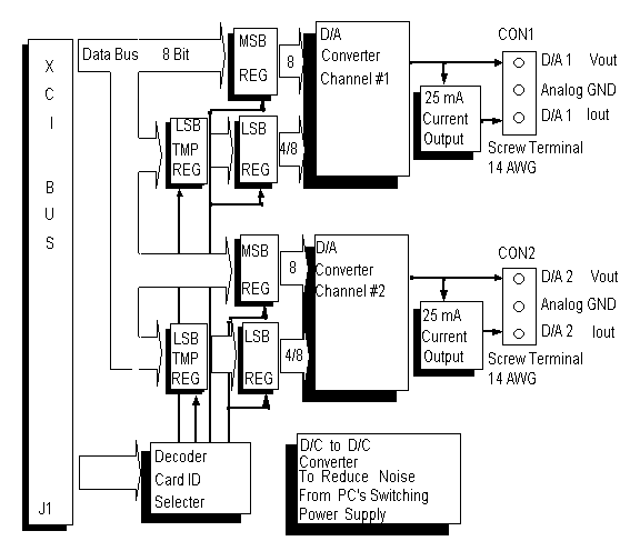
Data Register -
The XC-DA12(16) uses 4 data registers or ports. The ports are
base+0 through base+3.
Using 2 ports per channel enables the user to send a 12-bit or
16-bit word to the D/A converter using an 8-bit bus without
getting glitches on the output.
Here is an example of the data register scheme. Say a user
wishes to convert the digital value from 1AFH to 1B0H to an
analog value in the 12-bit D/A conversion. Using the standard
approach of sending 8 bits at a time would result in a glitch
on the output at these digital value 1AFH-1A0H-1B0H (sending
LSB first, then MSB) or 1AFH-1BFH-1B0H (sending MSB first,
then LSB). However, using the XC-DA12 one would write the 0H
(4 least significant bits) to the temporary register (base+0
for channel 1 and base+2 for channel 2). Next the user would
write 1BH (8 most significant bits) to the D/A O/P (base+1 for
channel 1 and base+3 for channel 2). Upon writing the MSB to
base+1, the data in the temporary register is automatically
sent to the output, thus, both MSB and LSB arrive at the D/A
simultaneously. (i.e. no glitch)
D/A conversion -
D/A conversion is accomplished using a 12 or 16 bit D/A
conversion chip. The 12-bit or 16-bit words are sent from the
data bus and a temporary register simultaneously. This
enables a 12-bit or 16-bit word to be sent from an 8-bit data
bus without getting odd glitches on the output. (See data
register section)
Voltage ranges -
The output from the D/A converter can be configurred for
different voltage ranges by using an on-board jumper. (JP3
for D/A1, JP5 for D/A2)The jumpers allow a user to decide on 4
different voltage ranges; they are -10V to +10V: -5V to +5V:
0 to +10V: and 0 to +5V. One jumper controls the output to
be unipolar or bipolar, the other two jumpers control the
output to be 5V or 10V maximum.
Current Output -
The XC-DA12(16) provides 2 current outputs.
The signal connecter -
The signal connecter for D/A output signals is the 3 SIL 14
AWG screw terminal. Be sure to check the pin diagram before
using.
|